Difference between revisions of "PAL (Chip)"
Omega Haxors (talk | contribs) |
|||
| Line 14: | Line 14: | ||
Play a little with the 3 buttons and the PAL configuration to see how it works. | Play a little with the 3 buttons and the PAL configuration to see how it works. | ||
| − | + | [[File:PAL Color Map.png|thumb]] | |
| − | |||
| − | |||
| − | |||
| − | |||
| − | |||
| − | |||
| − | |||
| − | |||
| − | |||
| − | |||
| − | |||
| − | |||
| − | |||
| − | |||
| − | |||
| − | |||
| − | |||
[[Category:Digital chips]] | [[Category:Digital chips]] | ||
Revision as of 15:24, 31 August 2018
A Programmable Array Logic (PAL) is a programmable logic device semiconductors used to implement any logic function in only one digital circuit. The function is stateless, which means that no intermediate state is saved.
PAL devices consisted of a small PROM (programmable read-only memory) core and additional output logic used to implement particular desired logic functions with few components.
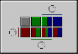
You can use PALs in order to implement any logic function you might need. The PAL chip offers an UI where it's logic function can be programmed very simple. The programming is made using a Karnaugh map. Basically you can specify for each possible state of the three inputs (2 ^ 3 = 8) the resulting output value. All 3 inputs are represented by bars and for all cells in the map that are covered by that bar, the corresponding input is considered as 1 (high).
Play a little with the 3 buttons and the PAL configuration to see how it works.
